
Place of Origin:
Shen,zhen China
Brand Name:
Sky Win
Certification:
IATF16949
Model Number:
PCBA-T0022
Contact Us
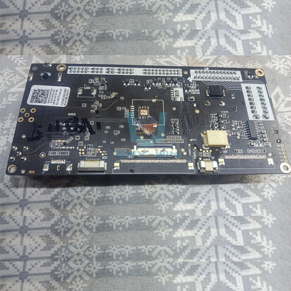
Through-Hole Assembly Multilayer Communication PCB Prototype Printed Circuit Boards
Communication PCB Assembly Description
PCB requirements in the field of communication can be divided into sub-fields such as communication equipment and mobile terminals. Among them, communication equipment mainly refers to the communication infrastructure used for wired or wireless network transmission, including communication base stations, routers, switches, backbone network transmission equipment, microwave transmission equipment, optical fiber to the home equipment
Communications PCB Material
Designing the best PCB solution for communications products requires careful selection of substrate laminates, prepregs, conductive layers, coatings and finishes. We use a range of materials specifically tailored to meet the electrical, mechanical and environmental performance standards required for these demanding applications.
Communication PCB Assembly Application
In the field of communication, communication PCB board is widely used in wireless network, transmission network, data communication. And fixed line broadband. Related PCB products include backboards, high-speed multilayer boards, high-frequency microwave boards, and multifunctional metal substrates.
PCB requirements in the field of communication are divided into subdivisions such as communication equipment and mobile terminals. Communication equipment is a communication infrastructure mainly used for wired or wireless network transmission. Including communication base stations, routers, switches, etc. Communication equipment mainly uses high-rise PCB boards, of which 8-16 layers account for about 42%. The mobile terminal is mainly HDI and flexible board.
Communications PCB Parameters
| Layer: | 8 layers |
| Surface: | HASL/OSP/ENIG/ImmersionGold/Flash Gold/Gold finger ect. |
| Copper thickness: | 0.25 Oz -12 Oz |
| Material: | FR-4,Halogen free,High TG,Cem-3,PTFE,Aluminum BT,Rogers |
| Board thickness | 0.1 to 6.0mm(4 to 240mil) |
| Minimum line width/space | 0.076/0.076mm |
| Minimum line gap | +/-10% |
| Outer layer copper thickness | 140um(bulk) 210um(pcb prototype) |
| Inner layer copper thickness | 70um(bulk) 150um(pcb protytype) |
| Min.finished hole size(Mechanical) | 0.15mm |
| Min.finished hole size (laser hole) | 0.1mm |
| Aspect ratio | 10:01(bulk) 13:01(pcb prototype) |
| Solder Mask Color | Green,Blue,Black,White,Yellow,Red,Grey |
| Tolerance of dimension size | +/-0.1mm |
| Tolerance of board thickness | <1.0mm +/-0.1mm |
| Tolerance of finished NPTH hole size | +/-0.05mm |
| Tolerance of finished PTH hole size | +/-0.076mm |
| Delivery time | Mass:10~12d/ Sample:5~7D |
![]()
Send your inquiry directly to us