|
|
|
|
|
|
Product Details:
Payment & Shipping Terms:
|
| Category: | Communications PCB | Surface Finishing: | HASL,OSP,ENIG,HASL Lead Free,Immersion Gold |
|---|---|---|---|
| Solder Mask: | Green/black/white/red/blue Etc. | PCB Assembly Method: | SMT,Through-hole |
| Usage: | OEM /ODM Electronics | PCB Glod Process: | Immerison Gold |
| PCB Material: | FR-4 | Request File: | Gerber Files(CAM, PCB, PCBDOC) |
| Min. Line Spacing: | 0.076mm | Min. Line Width: | 0.076mm |
| Min. Hole Size: | 0.20mm | Copper Thickness: | 1oz |
| Board Thickness: | 1.6mm | ||
| High Light: | 16 Layers Communication PCB Assembly,Green Communication PCB Assembly |
||
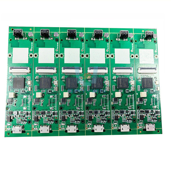
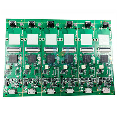
16 Layers FR4 HASL/ENIG Surface Green Soldermask Communication PCB Assembly
Communication PCB Assembly Services
With our rich experience and one-stop communications PCB assembly services, Sky-Win Technology helps clients develop reliable and innovative industrial products in a short time.
PCB Designing
Components Procurement
PCB Prototyping
PCB Assembly
Testing
Before delivery, we will apply a series of tests to check the quality and functionality of the PCBA, including circuit testing and 100% functional testing. We perform visual inspection, automated light inspection and automated X-ray inspection.
Communications PCB Assembly Category
| Application | Communication Product |
| PCB Material | FR4 |
| Dielectric constant | 4.2 |
| Outer copper thickness | 1OZ |
| Surface finishing | Immersion Gold |
| Min. line width | 0.076mm |
| Layer | 16 |
| Board thickness | 1.6mm |
| Inner copper thickness | 1OZ |
| Min. hole size | 0.2mm |
| Min. line spacing | 0.076mm |
| Feature | High Reliability ,High Precision |
Communication PCB Board Characteristics
In the field of communication electronics, communication PCB boards are widely used in wireless networks, transmission networks, and data communications. And fixed-line broadband. Related PCB products include baseboards, high-speed multilayer boards, high-frequency microwave boards and multifunctional metal substrates.
In order to cope with the outbreak of 5G communication, 5G air outlet has set off another wave of PCB, from 1G to 5G, the upgrade of communication technology: The upgrade of a new generation of communication technology has brought revolutionary changes to the terminal products and redefined the terminal products. Products, driven by the entire industrial chain reconstruction and great changes.
FAQ
1).Q: How to process it if i have no drawing?
A: Firstly let us know your detail requirements( if you have sample, please ship to us, we will copy it). Secondly We quote according to your requirements or our suggestions. Thirdly customer confirms the samples and places deposit for formal order. Fourthly We arrange the production.
2).Q: What is the MOQ and fastest deliver time?
A: 1 pcs prototype+air express like DHL/UPS/FedEx/TNT.
3).Q: What kind of files you need to PCBA quotations?
A: PCB files (Gerber), Bom list, XY Data (pick-N-place).
4).Q: Do you support OEM PCB services?
A: Yes, our R&D team is experienced and help you make your ideas come ture.
5).Q: Is it OK to print my logo on product?
A: Yes. Please inform us formally before our production and confirm the design firstly based on our sample.
![]()
Contact Person: Luna Xie
Tel: +8615814515236