
Place of Origin:
Shenzhen,China
Brand Name:
Sky-Win Technology
Certification:
IATF16949
Model Number:
T-PCBA19-20
Contact Us
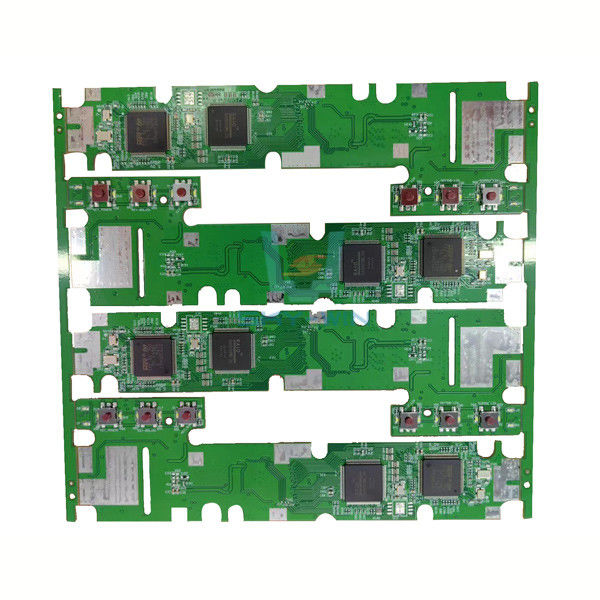
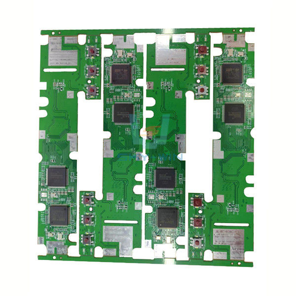
Fast PCB Fabrication Cost Reliable Printed Circuit Board With 10 Layer Pcb And Green Solder Mask
Fast PCB Fabrication Application
Printed circuitry is usually created on rigid PCB board (Printed Circuit Board) - a genericized term referring to a foundational element used in technology related products. PCB’s come in variety of physical form factors, each tailored to meet different requirements of a project. Let's look into four of the most popular:
Flexible PCB – often used in cell phones and small, handheld consumer electronics, this variation is characterized by its thin, flexible material, and its capability of “flexing” to fit into a confined physical space.
HDI PCB – or high density interconnect, also known as microvia PCB, has quickly become the premium choice for a variety of integrated circuit products. By decreasing the total surface area of a circuit and adding additional layers, HDI is able to create a level of precision and tight tolerance not yet seen.
Rigid Flex PCB – uses a combination of layers of flexible PCB and rigid PCB in its construction, so the board can be both rigid and flexible simultaneously. This form factor is often used in medical and aerospace applications due to its ability to withstand extreme temperature and pressure.
Rogers PCB – are especially popular when it comes to high power RF applications, allowing for advanced impedance matching techniques and superior electrical performance in comparison to most other types of PCB’s.
Ceramic PCB – these can come in either a rigid or a flex design, but what sets them apart is co-firing process which ensures a much more efficient heat dissipation. This form factor is popular in countries with hot climates, as it helps reduce the risk of overheating and damaging any fragile electronics.
PCB Fabrication Quotation Required Documents
1.Gerber files, PCB files, Eagle files or CAD files are acceptable
2. Detailed Bill of Materials (BOM)
3. Provide us with clear pictures of PCB or PCBA samples
4. Quantity and delivery requirements
5, PCBA test method to ensure 100% quality products.
6. If a functional test is required, a schematic file of the PCB design is required.
7. Sample (if available) for better sourcing
8. CAD file for case manufacture (if required)
9. Complete wiring and assembly drawings showing any special assembly instructions (if required)
PCB Fabrication PCB Design Engineering & PCB Production Services
Sky-Win Technology offers comprehensive PCB Design Engineering and PCB Production Services for the production of high quality and cost effective Printed Circuit Boards (PCBs). We provide technical support and services for PCB fabrication. Our goal is to help you with all aspects of the PCB fabrication process, from design to manufacturing and assembly. We offer support for all stages of the PCB fabrication process, including:
Our team of experienced engineers is available to provide you with the assistance you need to ensure the success of your PCB fabrication project. We also offer comprehensive technical documentation and online resources for your convenience.
If you have any questions about PCB fabrication or need help with a project, please contact us for more information. Our staff is always available to answer your questions and provide the necessary support.
| Article | Description | Capability | |
| Sercive | PCB and SMT assembly with one-stop service | ||
| Files we need | PCB: Gerber files(CAM, PCB, PCBDOC) | ||
| Components: Bill of Materials(BOM list) | |||
| Assembly: Pick-N-Place file | |||
| Material | Laminate materials | FR4, high TG FR4, high frequency, alum, FPC | |
| Board cutting | Number of layers | 1-32 | |
| Min.thickness for inner layers | 0.003”(0.07mm) | ||
| (Cu thickness are excluded) | |||
| Board thickness | Standard | (0.1-4mm±10%) | |
| Min. | Single/Double:0.008±0.004” | ||
| 4layer:0.01±0.008” | |||
| 8layer:0.01±0.008” | |||
| Bow and twist | 7/1000 | ||
| Copper weight | Outer Cu weight | 0.5-4 0z | |
| Inner Cu weight | 0.5-3 0z | ||
| Drilling | Min size | 0.0078”(0.2mm) | |
| Drill deviation | ±0.002″(0.05mm) | ||
| PTH hole tolerance | ±0.002″(0.005mm) | ||
| NPTH hole tolerance | ±0.002″(0.005mm) | ||
| Solder mask | Color | Green,white,black,red,blue… | |
| Min solder mask clearanace | 0.003″(0.07mm) | ||
| Thickness | (0.012*0.017mm) | ||
| Silkscreen | Color | white,black,yellow,blue… | |
| Min size | 0.006″(0.15mm) | ||
| E-test | Function Test | 100% Functional test | |
| PCBA Testing | X-ray,AOI Test,Functional test | ||
| Pcb assembly | one-stop service electronic manufacxturer service | ||
| Component sourcing | Yes | ||
| Certificate | IATF16949,ROHS,UL | ||
| Delivery time: | PCB | 3-12days | |
| PCBA | 8-20days | ||
| Tolerance of pcb | ±5% | ||
| Max size of finish board | 450*450mm | ||
| MOQ | NO MOQ (1pcs) | ||
| Surface Finish | HASL,ENIG,immersion silver,immersion tin,OSP… | ||
| PCB outline | Square,circle,irregular(with jigs) | ||
| package | QFN,BGA,SSOP,PLCC,LGA | ||
![]()
![]()
Send your inquiry directly to us