
Place of Origin:
Shenzhen,China
Brand Name:
Sky-Win Technology
Certification:
IATF16949
Model Number:
SMT-PCBA-2122
Contact Us
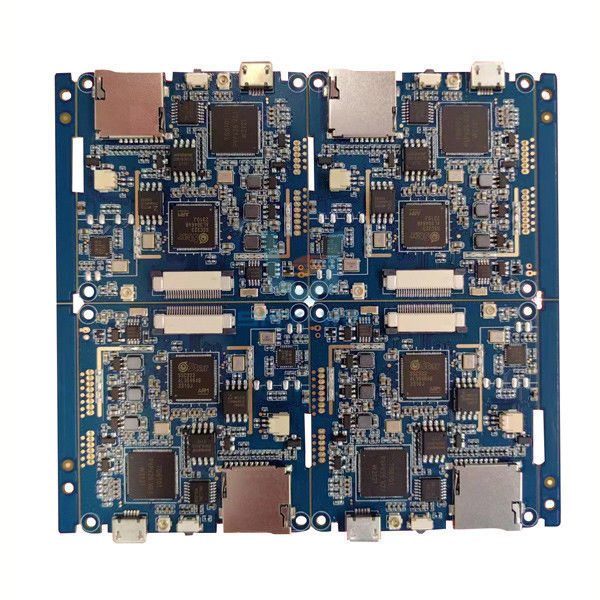
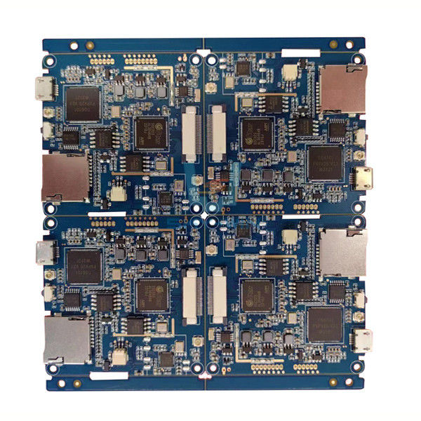
Engineering Design FR-4 Blue Pcb Assembly Service Using Surface Finish Immersion Gold With Function Test
Comprehensive Printed Circuit Board Assembly and Manufacturing Services
Shenzhen Skywin—Offering Comprehensive Printed Circuit Board Assembly and Manufacturing Services
Shenzhen Skywin provides a full range of printed circuit board assembly and manufacturing services that range from prototyping to production, to even repair. Our PCB assembly services involve designing, prototyping, new product introduction (NPI), supplying chain management, and assembling a comprehensive range of printed circuit boards with all necessary industry standards and RoHS complications.
Furthermore, we offer BGA reworking, conformal coating, IC programming, X-ray inspection, in-circuit testing (ICT), automated optical inspection, cable and wire harness assembly, and Box Build assembly as well. As an exclusive component of our PCB assembly services, we also provide samples of prototype assemblies, which customers can look over and accurately get a sense of what the ultimate assembly should look like. This ensures mistakes in design are amended in advance and underlying production costs are reduced.
Printed Circuit Board Assembly Technical Capabilities
| Article | Description | Capability | |
| Sercive | PCB and SMT assembly with one-stop service | ||
| Files we need | PCB: Gerber files(CAM, PCB, PCBDOC) | ||
| Components: Bill of Materials(BOM list) | |||
| Assembly: Pick-N-Place file | |||
| Material | Laminate materials | FR4, high TG FR4, high frequency, alum, FPC | |
| Board cutting | Number of layers | 1-32 | |
| Min.thickness for inner layers | 0.003”(0.07mm) | ||
| (Cu thickness are excluded) | |||
| Board thickness | Standard | (0.1-4mm±10%) | |
| Min. | Single/Double:0.008±0.004” | ||
| 4layer:0.01±0.008” | |||
| 8layer:0.01±0.008” | |||
| Bow and twist | 7/1000 | ||
| Copper weight | Outer Cu weight | 0.5-4 0z | |
| Inner Cu weight | 0.5-3 0z | ||
| Drilling | Min size | 0.0078”(0.2mm) | |
| Drill deviation | ±0.002″(0.05mm) | ||
| PTH hole tolerance | ±0.002″(0.005mm) | ||
| NPTH hole tolerance | ±0.002″(0.005mm) | ||
| Solder mask | Color | Green,white,black,red,blue… | |
| Min solder mask clearanace | 0.003″(0.07mm) | ||
| Thickness | (0.012*0.017mm) | ||
| Silkscreen | Color | white,black,yellow,blue… | |
| Min size | 0.006″(0.15mm) | ||
| E-test | Function Test | 100% Functional test | |
| PCBA Testing | X-ray,AOI Test,Functional test | ||
| Pcb assembly | one-stop service electronic manufacxturer service | ||
| Component sourcing | Yes | ||
| Certificate | IATF16949,ROHS,UL | ||
| Delivery time: | PCB | 3-12days | |
| PCBA | 8-20days | ||
| Tolerance of pcb | ±5% | ||
| Max size of finish board | 450*450mm | ||
| MOQ | NO MOQ (1pcs) | ||
| Surface Finish | HASL,ENIG,immersion silver,immersion tin,OSP… | ||
| PCB outline | Square,circle,irregular(with jigs) | ||
| package | QFN,BGA,SSOP,PLCC,LGA | ||
| Sub-assembly | Plastic,metal,screen | ||
PCB Assembly Service Technical Support and Service
We provide comprehensive technical support and service for our PCB Assembly Service. Our team of experts is available to answer any questions you have about our PCB Assembly Service and provide detailed guidance and assistance.
We provide technical support for all aspects of the PCB Assembly Service, including design, fabrication, assembly, testing, and troubleshooting. Our team of experts can provide detailed information on the components and materials used in the PCB Assembly Service, as well as any other information you may need to make an informed decision.
We also provide assistance with installation and setup of the PCB Assembly Service. Our team of experts can provide step-by-step instructions on how to install and use the PCB Assembly Service and can provide help in troubleshooting any issues you may encounter.
If you have any questions or need assistance with our PCB Assembly Service, please contact us and we will be more than happy to help.
PCB Assembly Service Packaging and Shipping
When shipping PCB assemblies, special care must be taken to ensure that the assemblies arrive in the same condition as when they were shipped. The assemblies must be packaged in appropriate containers and materials that will protect them from damage during transit. All necessary paperwork must also be included in the shipment and any special instructions must be clearly indicated.
The type of packaging used for PCB assemblies is highly dependent on the size and shape of the assemblies as well as the carrier that will be used for the shipment. Packaging materials such as bubble wrap, foam, and cardboard can be used to provide a cushion for the assemblies and help prevent them from shifting during transit. Additionally, the assemblies must be secured in the packaging to prevent them from slipping or becoming damaged.
The carriers used for shipping PCB assemblies must also be chosen carefully. Carriers such as FedEx and UPS are typically used for smaller shipments, while larger shipments may require the use of specialized carriers that are better equipped to handle heavier packages. Additionally, carriers must be chosen that are familiar with the proper handling of sensitive electronic components.
![]()
![]()
Send your inquiry directly to us