Place of Origin:
Shenzhen
Brand Name:
Sky-win
Certification:
IATF16949/ROHS
Model Number:
PCBA-3435
Contact Us
Double Sided PCB Copper Thickness 1/2 Oz 6 Oz With Highly Customizable PCB Prototype HASL Lead Free
Printed Circuit Board Assembly Description
Printed Circuit Board (PCB) assembly is an essential phase in the manufacturing of electronicscircuits and devices. It is key for better performance, good reliability, and functionality of electronics devices. Let us talk about PCB definition, assembly process, and best considerations.
Printed circuit board is the primary building block of any electronics device and circuit. It serves as a connector to link different electronics components. PCB designing and manufacturing in today’s modern technology are highly important in electronics circuits design. PCB gives the heart and soul to all electronic circuit designs. It helps us to create the physical form of our electronics circuits. As PCB is in charge of developing electrical connections among parts and allowing a device to communicate with the external environment, it's clear that only minimal design mistakes could cause further delays or expenses in manufacturing.
Advanced design tools have been instrumental in lowering production costs for PCB manufacturers. Nevertheless, higher manufacturing expenses may be incurred due to faults in PCB design. It's significant to understand that even for experienced PCB designers, errors may happen. That is why adhering to simple guidelines is suggested in order to avoid the ten most normal design mistakes, which we will address shortly.
PCB Prototype Assembly Features
We offer a range of printed circuit board engineering services, including design for manufacturability (DFM) and design for testing (DFT) prototype PCB assemblies. We also conduct process failure mode effects analysis (PFMEA) and create control plans. As well as these, we provide new product introduction (NPI) projects.
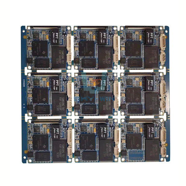
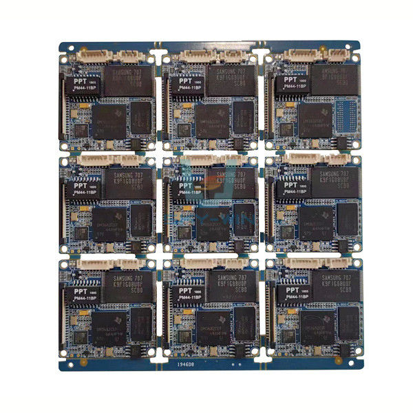
For our prototype PCB assembly services, we are specialized in single-sided and double-sided surface mount PCB assemblies with different specifications and selective soldering. We also deal with mixed assemblies, which contains both through-hole and SMT parts, as well as electro-mechanical assemblies.
Apart from fabrication, PCBA testing is also conducted in our facility with a large set of equipment. This setup allows us to perform various testing procedures, such as flying probe testing, functional testing, FPGA and micro-controller testing, HALT and HASS/HASS testing as well as impedance and thermal profiling.
PCB Prototype Assembly Parameters
|
PCB Item |
Technical Parameters |
|---|---|
|
Prototype PCB Assembly |
Components: SMD, Through Hole |
|
Highly customizable, fast delivery time, 100% quality guarantee. |
Customizable product design, fast delivery time, 100% quality guarantee. |
Applications For PCB Prototype Assembly
Sky-win's Prototype PCB Assembly is the perfect choice for fast turnaround and top-level quality assurance. It is certified with IATF16949/ROHS and has a minimum order quantity of 1 pcs. The price is negotiable, and the package comes in cartons. The delivery time is 5-8 work days of turnkey pcb assembly, and the payment terms are T/T or Western Union. It has a strong production capacity of 50000 pcs per months. The board thickness ranges from 0.4-3.2mm, and the copper thickness is from 1/2 Oz to 6 Oz. It supports surface finishes like HASL, ENIG, OSP, Immersion Silver, and Gold Finger, as well as solder mask colors like green, blue, white, black, and red. Most importantly, it has high reliability, fast delivery time, high density component support, and strong scalability. Sky-win's Prototype PCB Assembly is the perfect choice for all your needs!
Sky-win promises quality assurance in our Prototype PCB Assembly. In order to guarantee the best performance, the highest standards are applied in the production process.
![]()
![]()
Send your inquiry directly to us