
Place of Origin:
Shenzhen
Brand Name:
Sky-win
Certification:
IATF16949/ROHS
Model Number:
Prototype-Pcb Assembly -08-9
Contact Us
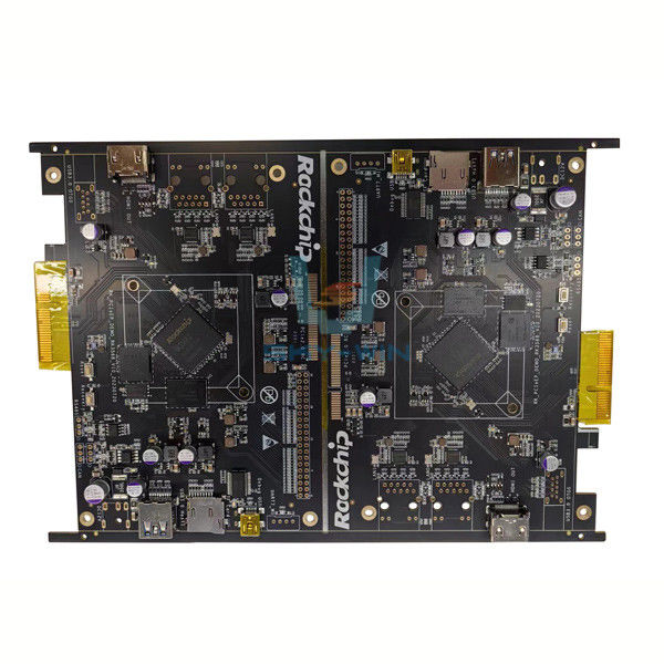
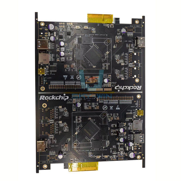
FR-4 Material PCB Assembly Min. Line Spacing 0.1mm Multi-Layer Prototype PCB Assembly With OSP Surface Finish
Prototype PCB Assembly
Printed circuit board assembly is an important step in the creation of electronics circuits and devices. It is essential for greater performance, reliability, and functionality. Due to its importance, let's take a closer look at what printed circuit board (PCB) is, how it's assembled, and the best considerations when designing one.
The PCB is the basic building block of any configuration and works as the connection hub between different electronics components. Today, PCBs are used across all industries, helping in the design of electronics circuits. They are, in effect, the soul and heart of all electronics circuits as they form the physical structure.
If the design of a PCB is not up to par, this may lead to delays, additional expenses during manufacturing, malfunctions, and complete circuit failures. Advanced design tools have assisted in reducing production costs, however, mistakes in the design phase can negate this. To avoid these mistakes, manufacturers should adhere to simple guidelines and take note of the most common design errors.
Features Of Prototype PCB Assembly
Printed Circuit Board Engineering Services
We provide specialized services for prototype PCB assemblies, designed to suit both design for manufacturability (DFM) and design for testing (DFT). For projects that require it, we can also apply process failure mode effects analysis (PFMEA) and devise control plans.
Prototype PCB Assembly Services
Our services cover a broad range of prototype PCB assembly operations that include both single-sided and double-sided surface mount PCB assemblies in different specifications along with plated through hole assembly with selective soldering.
We also deal with mixed assemblies, which involve both through-hole and surface-mount technology (SMT) along with electromechanical assemblies. Plus, we provide new product introduction (NPI) services.
PCBA Testing
We have invested in several test fixtures and equipment to ensure the quality of PCBA. We have our in-house facility to conduct all functional testing that covers flying probe testing, boundary testing, functional testing at both board and system level.
Prototype PCB Assembly Technical Parameters
|
Parameters |
Description |
|---|---|
| Board Type | Single Sided, Double Sided, Multi-Layer |
| Components | SMD, Through Hole |
| Min. Line Width | 0.1mm |
| Testing | Flying Probe, AOI, X-Ray |
| Silkscreen Color | White, Black, Yellow |
| Board Thickness | 0.4-3.2mm |
| Board Size | Customized |
| Min. Line Spacing | 0.1mm |
| Solder Mask Color | Green, Blue, White, Black, Red |
| Surface Finish | HASL, ENIG, OSP, Immersion Silver, Gold Finger |
| High Reliability | Yes |
| High Density Component Support | Yes |
| Strong Scalability | Yes |
| Highly Customizable | Yes |
Prototype PCB Assembly Applications
Sky-win Prototype PCB Assembly, with its model number of IATF16949/ROHS certification, is a high-reliability and high-density component support product with strong scalability that can meet the needs of customers in various industries. It is widely used for multi-layer PCB support and it can be customized to meet the specific requirements of customers. The minimum order quantity of this product is 1 pcs and the price is negotiable. It is packaged in cartons and the delivery time is 5-8 work days of turnkey pcb assembly. The payment terms are T/T or Western Union and the supply ability is 50000 pcs per months. The surface finish includes HASL, ENIG, OSP, Immersion Silver, Gold Finger and the silkscreen color is available in white, black and yellow. The copper thickness ranges from 1/2 Oz to 6 Oz and the board thickness is 0.4-3.2mm.
Prototype PCB Assembly Packaging and Shipping
Once the PCBA passes all inspections and tests, it is packaged for shipment. Packaging is designed to protect the components and PCB during transportation and storage.
![]()
![]()
Send your inquiry directly to us