Place of Origin:
Shen,zhen China
Brand Name:
Sky Win
Certification:
IATF16949
Model Number:
PCBA-T23
Contact Us
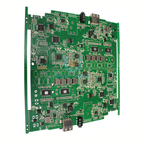
8 Layers FR4 Printed Circuit Board Gerber File For Communication PCB Assembly Network Communication
Communications Application
In the field of communication, communication PCB board is widely used in wireless network, transmission network, data communication. And fixed line broadband. Related PCB products include backboards, high-speed multilayer boards, high-frequency microwave boards, and multifunctional metal substrates.
PCB requirements in the field of communication are divided into subdivisions such as communication equipment and mobile terminals. Communication equipment is a communication infrastructure mainly used for wired or wireless network transmission. Including communication base stations, routers, switches, etc. Communication equipment mainly uses high-rise PCB boards, of which 8-16 layers account for about 42%. The mobile terminal is mainly HDI and flexible board.
Communications PCB Parameters
| Layer: | 8 layers |
| Surface: | HASL/OSP/ENIG/ImmersionGold/Flash Gold/Gold finger ect. |
| Copper thickness: | 0.25 Oz -12 Oz |
| Material: | FR-4,Halogen free,High TG,Cem-3,PTFE,Aluminum BT,Rogers |
| Board thickness | 0.1 to 6.0mm(4 to 240mil) |
| Minimum line width/space | 0.076/0.076mm |
| Minimum line gap | +/-10% |
| Outer layer copper thickness | 140um(bulk) 210um(pcb prototype) |
| Inner layer copper thickness | 70um(bulk) 150um(pcb protytype) |
| Min.finished hole size(Mechanical) | 0.15mm |
| Min.finished hole size (laser hole) | 0.1mm |
| Aspect ratio | 10:01(bulk) 13:01(pcb prototype) |
| Solder Mask Color | Green,Blue,Black,White,Yellow,Red,Grey |
| Tolerance of dimension size | +/-0.1mm |
| Tolerance of board thickness | <1.0mm +/-0.1mm |
| Tolerance of finished NPTH hole size | +/-0.05mm |
| Tolerance of finished PTH hole size | +/-0.076mm |
| Delivery time | Mass:10~12d/ Sample:5~7D |
The PCBA Assembly Process For Communication Equipment Typically Includes The FollowingSteps
PCB design: The first step in PCBA assembly is to design the PCB according to the specifications and requirements of the communication equipment
Component selection: After the PCB design is complete, the next step is to select the components that will be used in the assembly. This typically includes components such as microprocessors, memory chips, radio frequency (RF) modules, and other electronic components.
PCB assembly: The selected components are then assembled onto the PCB using an automatic pickup and placement machine. Place the components onto the PCB and weld them into place using a reflow furnace.
Testing: After the PCB is assembled, the PCBA is tested to ensure that it meets the necessary performance and reliability standards. This includes functional, performance and durability testing.
Quality control: The final step in PCBA assembly is quality control, which includes checking the PCBA for defects and ensuring that it meets the necessary quality standards.
Communication PCB Assembly Manufacturer
Sky-win Technology Co, Ltd. was founded in Shenzhen in 2015. lt is a leading electronic manufacturingservices (EMS) provider in China. Sky-win is also a high-tech enterprise integrating R&D, production andsales of PCB&PABA products. Shenzhen Sky-win Technology Co., Ltd. has more than 100 employees,eading by core managers who have worked in PCB/PCBA industry companies for at least 15 years, andhave rich experience in PCB/PCBA products research and development, production and qualitymanagement.
![]()
Send your inquiry directly to us