Place of Origin:
Shenzhen,China
Brand Name:
Sky-Win Technology
Certification:
IATF16949
Model Number:
SMT-PCBA-050
Contact Us
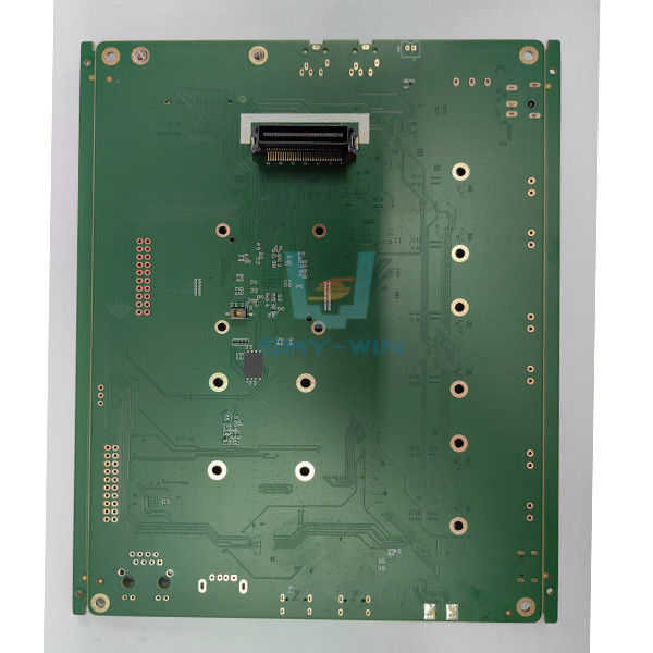
A client from the network communications sector required a specialized collaborator, known for their expertise and comprehensive capabilities, to assemble their printed circuit board (PCB) with meticulous attention to detail. The project called for precision and sophistication in assembly processes.
The PCB assembly was executed with cutting-edge automatic insertion machinery complemented by meticulous hand insertion methods. Precision was paramount, and each component was placed with exacting accuracy. To further ensure the integrity of the connections, hand soldering techniques were utilized with strict adherence to a lead-free solder standard.
Constructed from high-quality FR4 material, the board was designed to handle complex configurations. It boasted a total of 729 component placements, achieved through the use of sophisticated surface mount and through-hole mounting technologies. In terms of complexity, the multilayer board consisted of 8 distinct layers and was compatible with a variety of package sizes, including 0603. It also accommodated fine-pitch spacing that met the requirements of specified LGA, BGA, and QFN packages.
To guarantee the product met the highest quality standards, rigorous quality control measures were in place, including automated optical inspection (AOI) and comprehensive functionality testing. This thorough approach was not just about adhering to standards, it was about surpassing client expectations. Despite the complexity, the project was completed within an impressive 4 to 6-week timeframe.
Printed Circuit Boards (PCBs) stand as the cornerstone of modern communication devices, incorporating meticulously crafted multilayer High-Density Interconnect (HDI) boards. The dawn of the 5G era beckons a surge in demand for PCBs that exemplify exceptional stability, adaptability, and user-friendliness during both manufacturing and assembly processes.
Skywin positions itself at the forefront of this technological evolution, offering expeditious, turnkey solutions for PCB manufacturing and assembly. Our services extend to an array of communication tools, including base station apparatus, wireless machinery, and handheld digital devices, among others.
Our dedication to excellence is showcased in the 5G smartphones that we have crafted for our clientele. These devices are composed of Class-A substrates and utilize purely original components. They are constructed following the RoHS & REACH regulations, attesting to our commitment to sustainability and consumer safety.
In their quest for compliance with the stringent standards set by local telecommunications entities, our products have undergone rigorous inspections, triumphantly securing expedited market entry. This pivotal step has catalyzed a marked uptick in sales, as recognition of product quality resonates with a growing consumer base.
| Assembly Process | Double-sided Mounting |
| Surface | HASL/OSP/ENIG/ImmersionGold/Flash Gold/Gold finger ect. |
| Copper thickness | 0.25 Oz -12 Oz |
| Material | FR-4,Halogen free,High TG,Cem-3,PTFE,Aluminum BT,Rogers |
| Board thickness | 0.1 to 6.0mm(4 to 240mil) |
| Minimum line width/space | 0.076/0.076mm |
| Minimum line gap | +/-10% |
| Outer layer copper thickness | 140um(bulk) 210um(pcb prototype) |
| Inner layer copper thickness | 70um(bulk) 150um(pcb protytype) |
| Min.finished hole size(Mechanical) | 0.15mm |
| Min.finished hole size (laser hole) | 0.1mm |
| Aspect ratio | 10:01(bulk) 13:01(pcb prototype) |
| Solder Mask Color | Green,Blue,Black,White,Yellow,Red,Grey |
| Tolerance of dimension size | +/-0.1mm |
| Tolerance of board thickness | <1.0mm +/-0.1mm |
| Tolerance of finished NPTH hole size | +/-0.05mm |
| Tolerance of finished PTH hole size | +/-0.076mm |
| Delivery time | Mass:10~12d/ Sample:5~7D |
Q1: What is the brand name of the Communication PCB Assembly product?
A1: The brand name of the product is Sky-Win Technology.
Q2: Can you provide the model number for the Communication PCB Assembly?
A2: Yes, the model number is SMT-PCBA-050.
Q3: Where is the Communication PCB Assembly manufactured?
A3: The Communication PCB Assembly is manufactured in Shenzhen, China.
Q4: What certifications does the Communication PCB Assembly have?
A4: The Communication PCB Assembly is certified with IATF16949.
Q5: What is the minimum order quantity for the Communication PCB Assembly?
A5: The minimum order quantity for the Communication PCB Assembly is 10 units.
Q6: How is the Communication PCB Assembly priced?
A6: The price of the Communication PCB Assembly is subject to negotiation.
Q7: What are the packaging details for the Communication PCB Assembly?
A7: The Communication PCB Assembly is packaged in cartons.
Q8: What is the delivery time for the Communication PCB Assembly?
A8: The delivery time for the Communication PCB Assembly is 5-10 working days.
Q9: What are the payment terms for the Communication PCB Assembly?
A9: The payment terms for the Communication PCB Assembly are L/C, D/A, D/P, T/T.
Q10: What is the supply ability for the Communication PCB Assembly?
A10: The supply ability for the Communication PCB Assembly is 100,000 pcs.
![]()
Send your inquiry directly to us