
Place of Origin:
Shenzhen,China
Brand Name:
Sky-Win Technology
Certification:
IATF16949
Model Number:
T-PCBA29
Contact Us
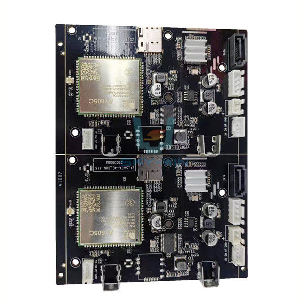
Manufacturing Of HDI PCB Electronic Products PCB Assembly For Smart Phone
Electronic PCB Assembly Capabilities
PCB Circuit component
Surface mount technology
Through hole plate assembly
Dual panel assembly and mixed assembly technology
In addition, many other types of electronic components
Electronic PCB Assembly Technical Parameters
|
Technical Parameter |
Description |
|---|---|
|
Solder Mask |
Green, White, Black, Etc. |
|
Min. Line Width/Space |
3/3mil |
|
Max. Board Size |
510*610mm |
|
Type |
PCB Assembly |
|
Copper Thickness |
1-6oz |
|
Product Name |
Electronic PCB Assembly |
|
Material |
FR4, Aluminum, Rogers, Etc. |
|
Layer |
1-20 Layers |
|
Silkscreen |
White, Black, Yellow, Etc. |
|
Surface treatment |
HASL;LF HASL;ENIG;Immersion Silver;Immersion Tin;Gold Finger;Flash Gold;OSP |
| Turnaround time | 1-4 days for only PCB assembly 9-15 days for full turn-key PCB assembly |
| Design file format | Gerber RS-274X, 274D, Eagle and AutoCAD's DXF, DWG BOM (Bill of Materials) (.xls, .csv, . xlsx) Centroid(Pick-N-Place/XY file) |
The Benefits of HDI For Electronic PCB Assembly
Improved electrical performance: Smaller components used on HDI boards have shorter internal wire lengths. This allows for shorter rise times and lower power requirements compared to larger alternative packages.
Reduce the PCB size. HDI creates a path to miniaturization of PCB designs through the "through hole in the pad" technology.
Improve reliability by enhancing technology rather than compromising existing design rules.
Get design choices when it comes to BGA layouts with minimal spacing.
Increased thermal reinforcement.
Increase interconnection density by reducing plating through holes, pad size and conductor size.
Using HDI (High Density Interconnect) to achieve higher wiring density per unit area. They are ideal for using smaller, future-proof components at scale. They provide faster signal transmission and significantly reduce signal loss and cross delay, making them ideal for shrinking PCB sizes.
FAQ:
Q: What is Electronic PCB Assembly?
A: Electronic PCB Assembly is the process of assembling Printed Circuit Boards (PCBs) with electrical components to form a functioning electronic circuit.
Q: Where is Electronic PCB Assembly from?
A: Electronic PCB Assembly is from Shenzhen,China. Sky-Win Technology is the brand name of this product.
Q: How long does it take to deliver Electronic PCB Assembly?
A: It usually takes 5-10 working days to deliver Electronic PCB Assembly from Sky-Win Technology.
Q: What are the payment terms for Electronic PCB Assembly?
A: Sky-Win Technology accepts L/C, D/A, D/P, T/T as payment terms for Electronic PCB Assembly.
Q: How many Electronic PCB Assemblies can be supplied?
A: Sky-Win Technology can supply up to 100000 pcs of Electronic PCB Assembly.
![]()
Send your inquiry directly to us