
Place of Origin:
China
Brand Name:
Sky Win
Certification:
IATF16949
Model Number:
001
Contact Us
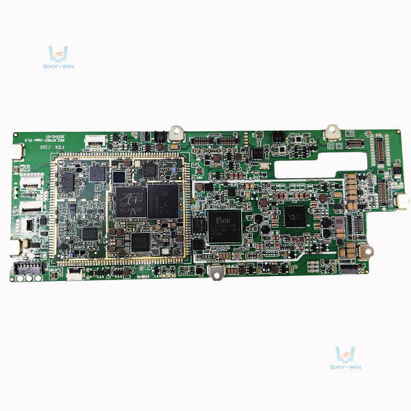
5G Communication PCB Assembly 1OZ Copper Prototype PCB Fabrication PCB Design
5G communication to PCB processing technology
1. Material requirements: A very clear direction for 5G communication PCB is high-frequency high-speed materials and boards.
2 For the requirements of quality monitoring, due to the improvement of 5G signal rate, the deviation of the board has a greater impact on signal performance, which requires the production deviation control of the board to be stricter, and the existing mainstream board process and equipment update is not big, which will become the bottleneck of future technological development.
3. Process requirements: The functional improvement of 5G-related applications will increase the demand for high-density PCBS, and HDI will also become an important technical field.
4. Requirements for PCB design; The selection of plates should meet the requirements of high frequency and high speed, clear resistance matching, cascade planning, wiring room/etc., to meet the signal integrity requirements, which can be started from the six aspects of loss, embedding, high frequency phase/amplitude, mixed pressure, heat dissipation, PIM.
5. Requirements for equipment and instruments: high-precision equipment and pre-treatment line with less coarsing of copper surface are currently ideal processing equipment, and test equipment is passive intermodulation tester, flying needle impedance tester, loss test equipment, etc. Precision graphics transfer and vacuum etching equipment, detection equipment that can monitor and feedback data changes in real time, line width and close spacing, electroplating equipment with good uniformity, high-precision laminating equipment, etc., can also meet the production needs of 5G communication PCB.
Communications PCB Parameters
| Application field | 5G Communication |
| Basic material | FR-4 |
| Dielectric constant | 4.2 |
| Outer copper foil thickness | 1OZ |
| Inner Copper Foil Thickness | 1OZ |
| Min Hole Diameter | 0.2mm |
| PCB Glod process | Immerison Gold |
| Number of PCB layers | 16 layers |
| PCB Surface | Double Sided Board |
| Min line width | 0.076 mm |
| Minimum line spacing | 0.076 mm |
| Board thickness | 1.6 mm |
| Manufacturing quality system | IATF16949 |
| Feature | High reliability and precision |
Communication PCB Assembly Manufacturer
Shenzhen SKY-WIN Technology Co., Ltd was founded in February 2015, focusing on PCBA OEM/ODM one-stop service, solution customization, SMT patch, DIP plug-in, functional testing, assembly and other OEM/ODM services.
![]()
Send your inquiry directly to us