
Place of Origin:
Shenzhen
Brand Name:
Sky-Win
Certification:
IATF16949/ROHS
Model Number:
013 PCB Fabrication
Contact Us
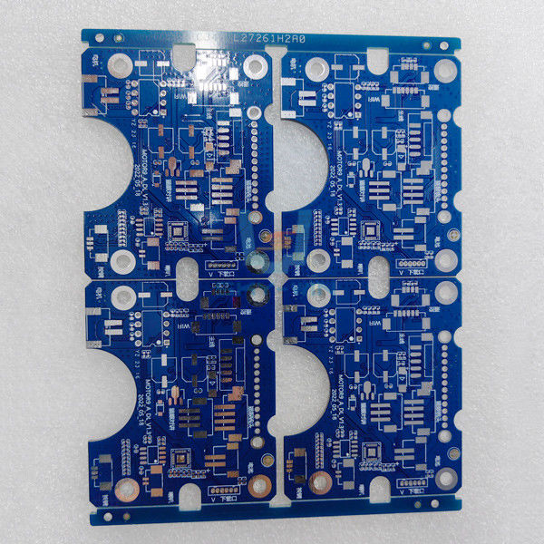
Timely Delivery For PCB Fabrication HDI Differential Impedance With Blue Soldermask
PCB Fabrication Service
1.Send Files (Gerber&BOM)
2.Quote In 24 Hours
3.Confirm The File and Order
4.PCB Fabrication
5.Components Procurement
6.Soldering,Testing Quality Control
7.Packaging&Delivery
1. HDI (High Density Interconnector)
HDI is the abbreviation of High Density Interconnector (High Density Interconnector) is a kind of (technology) for the production of printed circuit boards, and a circuit board with relatively high line distribution density using micro-blind buried hole technology. HDI is a compact product designed for small volume users.
2. Advantages
1). Can reduce the cost of PCB: when the density of PCB increases by more than eight layers, the cost can be greatly reduced by HDI.
2). Increase line density: the interconnection of traditional circuit boards and parts.
3). Better electrical performance and signal correctness
4). Good reliability
5). Can improve thermal properties
3. Application of HDI
Electronic design is constantly improving the performance of the whole machine, but also trying to reduce its size. In small portable products, from mobile phones to smart weapons, "small" is the constant pursuit. High-density integration (HDI) technology enables end-product designs to be more miniaturized while meeting higher standards of electronic performance and efficiency. *HDI is widely used in mobile phones, digital (camera) cameras, MP3, MP4, laptop computers, automotive electronics and other digital products, etc., high-end HDI board is mainly used in 3G mobile phones, advanced digital cameras, IC carrier board and so on.
PCB Assembly Technical Capabilities
| Article | Description | Capability | |
| Sercive | PCB and SMT assembly with one-stop service | ||
| Files we need | PCB: Gerber files(CAM, PCB, PCBDOC) | ||
| Components: Bill of Materials(BOM list) | |||
| Assembly: Pick-N-Place file | |||
| Material | Laminate materials | FR4, high TG FR4, high frequency, alum, FPC | |
| Board cutting | Number of layers | 1-32 | |
| Min.thickness for inner layers | 0.003”(0.07mm) | ||
| (Cu thickness are excluded) | |||
| Board thickness | Standard | (0.1-4mm±10%) | |
| Min. | Single/Double:0.008±0.004” | ||
| 4layer:0.01±0.008” | |||
| 8layer:0.01±0.008” | |||
| Bow and twist | 7/1000 | ||
| Copper weight | Outer Cu weight | 0.5-4 0z | |
| Inner Cu weight | 0.5-3 0z | ||
| Drilling | Min size | 0.0078”(0.2mm) | |
| Drill deviation | ±0.002″(0.05mm) | ||
| PTH hole tolerance | ±0.002″(0.005mm) | ||
| NPTH hole tolerance | ±0.002″(0.005mm) | ||
| Solder mask | Color | Green,white,black,red,blue… | |
| Min solder mask clearanace | 0.003″(0.07mm) | ||
| Thickness | (0.012*0.017mm) | ||
| Silkscreen | Color | white,black,yellow,blue… | |
| Min size | 0.006″(0.15mm) | ||
| E-test | Function Test | 100% Functional test | |
| PCBA Testing | X-ray,AOI Test,Functional test | ||
| Pcb assembly | one-stop service electronic manufacxturer service | ||
| Component sourcing | Yes | ||
| Certificate | IATF16949,ROHS,UL | ||
| Delivery time: | PCB | 3-12days | |
| PCBA | 8-20days | ||
| Tolerance of pcb | ±5% | ||
| Max size of finish board | 450*450mm | ||
| MOQ | NO MOQ (1pcs) | ||
| Surface Finish | HASL,ENIG,immersion silver,immersion tin,OSP… | ||
| PCB outline | Square,circle,irregular(with jigs) | ||
| package | QFN,BGA,SSOP,PLCC,LGA | ||
![]()
Send your inquiry directly to us