
Place of Origin:
Shenzhen
Brand Name:
Sky-Win
Certification:
IATF16949/ROHS
Model Number:
PCBA-30
Contact Us
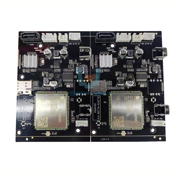
OEM Custom Max Finished Board Size 800*508mm Electronic PCB Fabrication OSP Multilayer PCB Assembly
Quick Turn PCB Fabrication Solutions
Sky-Win is a professional PCB manufacturer with more than 8 years of experience in 1-32 layer PCB production. We have the flexibility to quickly convert PCB prototypes to mass production.
We have the ability to quickly convert PCBS to meet your demanding project deadlines and the proper procedures to ensure your order is expedited throughout the process.
What is the PCB Fabrication Process?
The PCB fabrication process involves several steps to transform a design into a physical printed circuit board (PCB). Here is an overview of the typical PCB fabrication process:
1. Design: The process begins with designing the PCB layout using computer-aided design (CAD) software. This includes placing components, creating electrical connections, and defining the PCB's dimensions and layers.
2. Design Verification: Before fabrication, the design is verified for errors, such as incorrect connections or design rule violations. Design verification tools are used to ensure the design is ready for fabrication.
3. Gerber File Generation: The design files are converted into Gerber files, which are a standard format for PCB fabrication. These files define the copper traces, pads, and other features of the PCB.
4. Material Selection: The substrate material, often FR-4 fiberglass-reinforced epoxy, is chosen based on the PCB's requirements. Other materials, such as copper foil and solder mask, are also selected.
5. Layer Stackup: For multi-layer PCBs, the layer stackup is determined. It specifies the arrangement and order of the copper layers, insulating layers, and prepreg layers that make up the PCB.
6. Preparing the Substrate: The substrate material is prepared by cutting it to the required size and cleaning it to remove any contaminants.
7. Copper Cladding: Copper foil is laminated onto the substrate to form the conductive layers of the PCB. The copper foil is bonded to the substrate using heat and pressure.
8. Imaging and Etching: A photosensitive layer, called photoresist, is applied to the copper layers. The Gerber files are used to expose the photoresist in the desired circuit pattern using UV light. The exposed areas are chemically developed, and the unmasked copper is etched away to create the copper traces.
9. Drilling: Holes, known as vias, are drilled into the PCB to allow for component mounting and electrical connections between layers. These holes may be plated to ensure conductivity.
10. Plating and Surface Finish: The exposed copper surfaces are plated with a thin layer of a conductive metal, such as tin or gold, to protect them from oxidation and facilitate soldering. This plating process also helps establish electrical connections.
11. Solder Mask and Silk Screen: A solder mask layer is applied to cover the entire PCB, leaving only the copper pads exposed. This layer protects the copper traces and prevents solder bridges. A silk screen layer is applied to print component identifiers, logos, and other markings on the PCB.
12. Electrical Testing: The fabricated PCBs undergo electrical testing to ensure that the connections and circuitry meet the design specifications. This testing can include checks for continuity, resistance, and insulation between different layers.
Once the PCBs pass the testing phase, they are ready for component assembly, which involves soldering the electronic components onto the board using PCB assembly processes.
It's important to note that the specific details of the PCB fabrication process may vary depending on factors such as the complexity of the design, the desired specifications, and the chosen fabrication facility.
PCB Assembly Fabrication Capabilities
| Feature | Technical specification |
| PCB layer | 1-30 layers |
| Material | CEM-1, CEM-3 FR-4, FR-4 High TG |
| Board thickness | 0.2mm-6mm |
| Max.finished board size | 800*508mm |
| Min.drilled hole size | 0.25mm |
| min.line width | 0.075mm(3mil) |
| min.line spacing | 0.075mm(3mil) |
| Surface finish | HAL, HAL Lead free,Immersion Gold/ Silver/Tin,Hard Gold, OSP |
| Copper thickness | 0.5-4.0oz |
| Solder mask color | green/black/white/red/blue/yellow |
| Inner packing | Vacuum packing, Plastic bag |
| Outer packing | standard carton packing |
| Files we need | PCB: Gerber files(CAM, PCB, PCBDOC) Bill of Materials(BOM list) Assembly: Pick-N-Place file |
PCB Fabrication Lead Time
| Layer/Days | Sample(Normal) | Sample(Fast) | Mass Production |
| Single/Double | 2-3days | 24hours | 5-7days |
| Four Layer | 7-10days | 3days | 7-10days |
| Six Layer | 7-10days | 5days | 13-15days |
| Eight Layer | 15-20days | 7days | 15-20days |
Quick PCB Fabrication Services
24 hours quick turn PCB prototype
24x7 online technical sales service
Gerber file evaluation before production
FAQ
1).Q: How to process it if i have no drawing?
A: Firstly let us know your detail requirements( if you have sample, please ship to us, we will copy it). Secondly We quote according to your requirements or our suggestions. Thirdly customer confirms the samples and places deposit for formal order. Fourthly We arrange the production.
2).Q: What is the MOQ and fastest deliver time?
A: 1 pcs prototype+air express like DHL/UPS/FedEx/TNT.
3).Q: What kind of files you need to PCBA quotations?
A: PCB files (Gerber), Bom list, XY Data (pick-N-place).
4).Q: Do you support OEM PCB services?
A: Yes, our R&D team is experienced and help you make your ideas come ture.
5).Q: Is it OK to print my logo on product?
A: Yes. Please inform us formally before our production and confirm the design firstly based on our sample.
![]()
Send your inquiry directly to us