
Place of Origin:
Shenzhen
Brand Name:
Sky-Win
Certification:
IATF16949/ROHS
Model Number:
PCBA-027
Contact Us
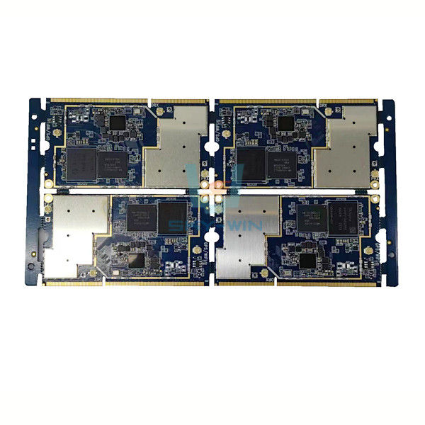
SMT DIP FR-4 Materials Black Color Use For Printed Circuit Boards Multilayer PCB Fabrication
PCB Fabrication
PCB fabrication, also known as PCB manufacturing or PCB production, is the process of manufacturing printed circuit boards (PCBs) that are used to mount and connect electronic components. It involves several steps to transform a design into a physical PCB.
The fabrication process typically starts with the design files, which include the layout and electrical connections of the PCB. These design files are then transferred to a fabrication facility, where the actual manufacturing takes place. Here are the main steps involved in PCB fabrication:
1. Substrate Preparation: The fabrication process begins with preparing the substrate material, usually a fiberglass-reinforced epoxy laminate called FR-4. The substrate is cut to the required size and cleaned to remove any impurities.
2. Layer Stackup: Multiple layers of copper foil are laminated onto the substrate to create a multi-layer PCB. The layers are aligned and pressed together under high temperature and pressure. Each layer has a specific pattern of copper traces and pads that form the electrical connections.
3. Imaging and Etching: A photosensitive layer called the photoresist is applied to the copper layers. The PCB design is transferred onto the photoresist using a UV light source and a specialized mask or film. The exposed areas of the photoresist are then chemically developed, revealing the copper traces. The unmasked copper is subsequently etched away using an etchant, leaving behind the desired circuit pattern.
4. Drilling: Holes for component mounting and electrical connections are drilled into the PCB. These holes, known as vias, are typically plated with copper to establish electrical connections between different layers of the PCB.
5. Plating and Surface Finish: The exposed copper surfaces are plated with a thin layer of a conductive metal, such as tin or gold, to protect them from oxidation and facilitate soldering. This plating process also helps establish electrical connections between components and the PCB.
6. Solder Mask and Silk Screen: A solder mask layer is applied to cover the entire PCB, leaving only the copper pads exposed. This layer protects the copper traces from environmental factors and prevents solder bridges during assembly. Additionally, a silk screen layer is applied to print component identifiers, logos, and other markings on the PCB.
7. Electrical Testing: The fabricated PCBs undergo rigorous electrical testing to ensure that the connections and circuitry meet the design specifications. This testing can include checks for continuity, resistance, and insulation between different layers.
Once the PCBs pass the testing phase, they are ready for component assembly, which involves soldering the electronic components onto the board through PCB assembly processes.
PCB fabrication is a critical step in the manufacturing of electronic devices, as it determines the quality, reliability, and functionality of the final product.
Printed Circuit Board Fabrication Capability
| Article | Description | Capability | |
| Sercive | PCB and SMT assembly with one-stop service | ||
| Files we need | PCB: Gerber files(CAM, PCB, PCBDOC) | ||
| Components: Bill of Materials(BOM list) | |||
| Assembly: Pick-N-Place file | |||
| Material | Laminate materials | FR4, high TG FR4, high frequency, alum, FPC | |
| Board cutting | Number of layers | 1-32 | |
| Min.thickness for inner layers | 0.003”(0.07mm) | ||
| (Cu thickness are excluded) | |||
| Board thickness | Standard | (0.1-4mm±10%) | |
| Min. | Single/Double:0.008±0.004” | ||
| 4layer:0.01±0.008” | |||
| 8layer:0.01±0.008” | |||
| Bow and twist | 7/1000 | ||
| Copper weight | Outer Cu weight | 0.5-4 0z | |
| Inner Cu weight | 0.5-3 0z | ||
| Drilling | Min size | 0.0078”(0.2mm) | |
| Drill deviation | ±0.002″(0.05mm) | ||
| PTH hole tolerance | ±0.002″(0.005mm) | ||
| NPTH hole tolerance | ±0.002″(0.005mm) | ||
| Solder mask | Color | Green,white,black,red,blue… | |
| Min solder mask clearanace | 0.003″(0.07mm) | ||
| Thickness | (0.012*0.017mm) | ||
| Silkscreen | Color | white,black,yellow,blue… | |
| Min size | 0.006″(0.15mm) | ||
| E-test | Function Test | 100% Functional test | |
| PCBA Testing | X-ray,AOI Test,Functional test | ||
| Pcb assembly | one-stop service electronic manufacxturer service | ||
| Component sourcing | Yes | ||
| Certificate | IATF16949,ROHS,UL | ||
| Delivery time: | PCB | 3-12days | |
| PCBA | 8-20days | ||
| Tolerance of pcb | ±5% | ||
| Max size of finish board | 450*450mm | ||
| MOQ | NO MOQ (1pcs) | ||
| Surface Finish | HASL,ENIG,immersion silver,immersion tin,OSP… | ||
| PCB outline | Square,circle,irregular(with jigs) | ||
| package | QFN,BGA,SSOP,PLCC,LGA | ||
| Sub-assembly | Plastic,metal,screen | ||
PCB Fabrication Manufacturing Files
The complete set of files required to manufacture the PCB is generated from the ECAD software package. The following table outlines the important manufacturing documents required by customers to fabricate, verify, and test bare PCBs prior to assembly.
PCB files (Gerber)
Bom list
XY Data (pick-N-place)
Why Sky-win is an Excellent PCB Assembly Manufacturer?
1. Sky-win has high quality manufacturing capability: An excellent PCB assembly manufacturer should have high quality manufacturing capability to ensure the quality and reliability of PCBs.
2. Sky-win has good production process: There are good production process and standard operation procedures to ensure that every step of operation is strictly executed according to the requirements, thus reducing errors and defects in production.
3. Sky-win has excellent equipment and technology: We have advanced manufacturing equipment and technology to meet the needs of different PCBs, and we have certain technical strength and R&D capability.
4. Sky-win has excellent customer service: we are able to respond to customers' needs in a timely manner and provide excellent service and support, including pre-sales, in-sales and after-sales services.
5.Sky-win has reasonable price: provide reasonable price and cost-effective products, so that customers can reach a balance point between price and quality.
6. Sky-win keeps improving: constantly reviewing and improving itself and actively introducing new technologies, new techniques and new equipments to keep the competitiveness in the market.
To sum up, Sky-Win is an excellent PCB assembly manufacturer.
![]()
Send your inquiry directly to us