
Place of Origin:
Shen,zhen China
Brand Name:
Sky Win
Certification:
IATF16949
Model Number:
PCBA-T0022
Contact Us
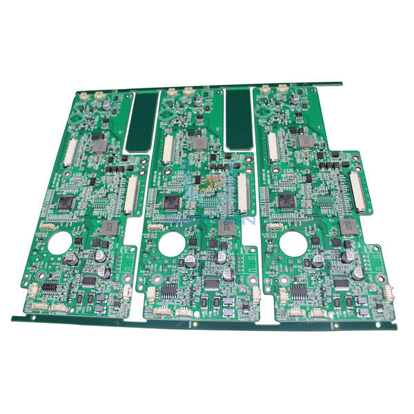
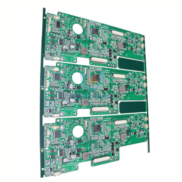
HASL Lead Free Multilayer Communication PCB Assembly Heavy Copper Impedance Control PCB 6mm
Communication PCB Assembly Description
With the rapid development of information and communication technology, electronic devices such as smart phones, wireless routers, base stations and other communication equipment have become an indispensable part of People's Daily life and work. The printed circuit boards in these devices are the basis for the assembly of components and integrated circuits, capable of transmitting high-speed signals and data that make communication possible.
Communication device PCBS use conductive copper traces etched from a copper-covered laminate to facilitate the interconnection between active and passive components. They provide the mechanical support and necessary electrical connections determined by the intended function of the device. But most importantly, PCBS designed for communication applications must transmit signals accurately and reliably between components without unacceptable loss or interference. This requires specialized materials and manufacturing processes to meet the unique needs of high-frequency communication electronics.
Communication PCB Assembly Application
In the field of communication, communication PCB board is widely used in wireless network, transmission network, data communication. And fixed line broadband. Related PCB products include backboards, high-speed multilayer boards, high-frequency microwave boards, and multifunctional metal substrates.
PCB requirements in the field of communication are divided into subdivisions such as communication equipment and mobile terminals. Communication equipment is a communication infrastructure mainly used for wired or wireless network transmission. Including communication base stations, routers, switches, etc. Communication equipment mainly uses high-rise PCB boards, of which 8-16 layers account for about 42%. The mobile terminal is mainly HDI and flexible board.
Communications PCB Parameters
| Layer: | 8 layers |
| Surface: | HASL/OSP/ENIG/ImmersionGold/Flash Gold/Gold finger ect. |
| Copper thickness: | 0.25 Oz -12 Oz |
| Material: | FR-4,Halogen free,High TG,Cem-3,PTFE,Aluminum BT,Rogers |
| Board thickness | 0.1 to 6.0mm(4 to 240mil) |
| Minimum line width/space | 0.076/0.076mm |
| Minimum line gap | +/-10% |
| Outer layer copper thickness | 140um(bulk) 210um(pcb prototype) |
| Inner layer copper thickness | 70um(bulk) 150um(pcb protytype) |
| Min.finished hole size(Mechanical) | 0.15mm |
| Min.finished hole size (laser hole) | 0.1mm |
| Aspect ratio | 10:01(bulk) 13:01(pcb prototype) |
| Solder Mask Color | Green,Blue,Black,White,Yellow,Red,Grey |
| Tolerance of dimension size | +/-0.1mm |
| Tolerance of board thickness | <1.0mm +/-0.1mm |
| Tolerance of finished NPTH hole size | +/-0.05mm |
| Tolerance of finished PTH hole size | +/-0.076mm |
| Delivery time | Mass:10~12d/ Sample:5~7D |
Sky-Win PCB Specializes in Prototype and Low Volume PCB Assembly
![]()
Send your inquiry directly to us