
Place of Origin:
Shenzhen,China
Brand Name:
Sky-Win Technology
Certification:
IATF16949
Model Number:
T-PCBA12
Contact Us
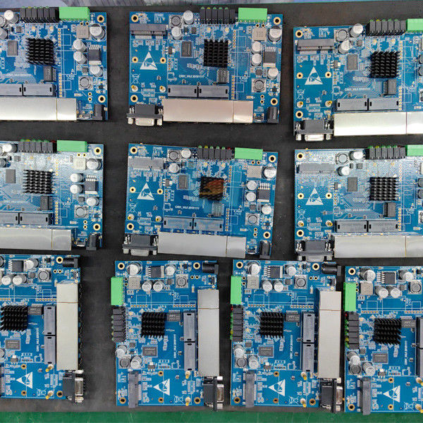
ROHS OSP ENIG 4mil Double Sided PCB Fabrication Immersion Tin One Stop PCB Service
PCB Fabrication Process
The PCB fabrication process involves several steps to transform a design into a physical printed circuit board (PCB). Here is an overview of the typical PCB fabrication process:
1. Design: The process begins with designing the PCB layout using computer-aided design (CAD) software. This includes placing components, creating electrical connections, and defining the PCB's dimensions and layers.
2. Design Verification: Before fabrication, the design is verified for errors, such as incorrect connections or design rule violations. Design verification tools are used to ensure the design is ready for fabrication.
3. Gerber File Generation: The design files are converted into Gerber files, which are a standard format for PCB fabrication. These files define the copper traces, pads, and other features of the PCB.
4. Material Selection: The substrate material, often FR-4 fiberglass-reinforced epoxy, is chosen based on the PCB's requirements. Other materials, such as copper foil and solder mask, are also selected.
5. Layer Stackup: For multi-layer PCBs, the layer stackup is determined. It specifies the arrangement and order of the copper layers, insulating layers, and prepreg layers that make up the PCB.
6. Preparing the Substrate: The substrate material is prepared by cutting it to the required size and cleaning it to remove any contaminants.
7. Copper Cladding: Copper foil is laminated onto the substrate to form the conductive layers of the PCB. The copper foil is bonded to the substrate using heat and pressure.
8. Imaging and Etching: A photosensitive layer, called photoresist, is applied to the copper layers. The Gerber files are used to expose the photoresist in the desired circuit pattern using UV light. The exposed areas are chemically developed, and the unmasked copper is etched away to create the copper traces.
9. Drilling: Holes, known as vias, are drilled into the PCB to allow for component mounting and electrical connections between layers. These holes may be plated to ensure conductivity.
10. Plating and Surface Finish: The exposed copper surfaces are plated with a thin layer of a conductive metal, such as tin or gold, to protect them from oxidation and facilitate soldering. This plating process also helps establish electrical connections.
11. Solder Mask and Silk Screen: A solder mask layer is applied to cover the entire PCB, leaving only the copper pads exposed. This layer protects the copper traces and prevents solder bridges. A silk screen layer is applied to print component identifiers, logos, and other markings on the PCB.
12. Electrical Testing: The fabricated PCBs undergo electrical testing to ensure that the connections and circuitry meet the design specifications. This testing can include checks for continuity, resistance, and insulation between different layers.
Once the PCBs pass the testing phase, they are ready for component assembly, which involves soldering the electronic components onto the board using PCB assembly processes.
It's important to note that the specific details of the PCB fabrication process may vary depending on factors such as the complexity of the design, the desired specifications, and the chosen fabrication facility.
PCB Fabrication PCB Capability
| Item | Craft Ability |
| Surface Finish | HASL,Immersion Gold,Gold Plating,OSP,Immersion Tin,etc |
| Layer | 1-32 layers |
| Min.Line Width | 4mil |
| Min.Line Space | 4mil |
| Min.Space between Pad to Pad | 3mil |
| Min.Hole Diameter | 0.20mm |
| Min.Bonding Pad Diameter | 0.20mm |
| Max.Proportion of Drilling Hole and Board Thickness | 1:10 |
| Max.Size of Finish Board | 23inch*35inch |
| Rang of Finish Board′s Thickness | 0.21-3.2mm |
| Min.Thickness of Soldermask | 10um |
| Soldermask | Green,Yellow,Black,White,Red,transparent photosensitive solder mask,Strippable solder mask |
| Min.Linewidth of Idents | 4mil |
| Min.Height of Idents | 25mil |
| Color of Silk-screen | White,Yellow,Black |
Sky Win Technology's PCB Printed Circuit Board Fabrication
Sky Win PCB is one of the leading PCB prototype and turnkey manufacturers located in Shenzhen,China.
We have over than 8 years experience focusing on quick-turn-around printed circuit board manufacturing and can supply more than 50 countries with superior quality and high technology products.
We have complete quality and environment systems of PCB manufacturing, PCB design and SMT after few years of exploding and developing, and become a competitive PCB/PCBA supplier famous for her high technology and effective management.
![]()
Send your inquiry directly to us