
Place of Origin:
Shenzhen,China
Brand Name:
Sky-Win Technology
Certification:
UL, RoHS
Model Number:
PCBA
Contact Us
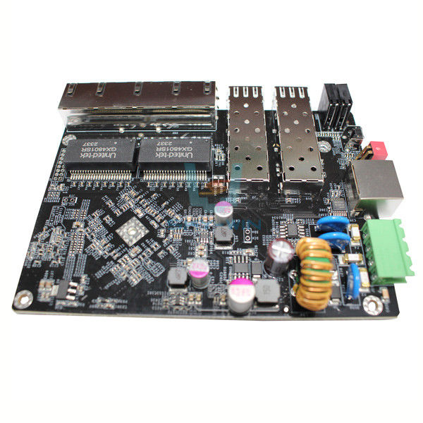
Quick Turn PCB Assembly SMT PCB Assembly SMT Stencil In PCB Design Surface Mount Technology
SMT Stencil Used In The PCB Design
Surface Mount Technology (SMT) templates are made of a thin, flexible material with openings corresponding to the pads of the components and holes in the PCB. The opening in the template allows conductive ink to flow during PCB etching. They are a great way to quickly and accurately apply solder paste to the pad on the circuit board. PCB templates help save money, improve quality and speed up the manufacturing process. Templates can be used for single or multi-layer boards, as well as multi-layer large boards. At Sky Win, we offer a wide range of rugged SMT Stencils to suit your specific manufacturing needs, manufacturing methods and components used in your board.
SMT PCB Assembly Features
Product Name: SMT PCB Assembly
Minimum Hole Distance: 0.2mm
Board Size: Customizable
Minimum Trace Distance: 0.1mm
Components: SMD, BGA, QFN, Etc.
Material: FR-4, Aluminum, Rogers, Etc.
Manufacturing Capabilities: PCB Assembly Manufacturer, Solder Paste Printing, Reflow Soldering, AOI, and X-ray Inspection
SMT PCB Assembly Technical Parameters
|
Parameters |
Specifications |
|---|---|
|
Minimum Hole Distance |
0.2mm |
|
Material |
FR-4, Aluminum, Rogers, Etc. |
|
Minimum Component Size |
0201 |
|
Board Thickness |
Customizable |
|
Minimum Hole Size |
0.2mm |
|
Minimum Silkscreen Clearance |
0.1mm |
|
Copper Thickness |
Customizable |
|
Minimum Solder Mask Clearance |
0.1mm |
|
Surface Finish |
HASL, ENIG, OSP, Etc. |
|
Product Type |
SMT PCB Assembly |
|
Ball Grid Array (BGA) |
Yes |
|
Gerber Files |
Yes |
|
Bill of Materials (BOM) |
Yes |
What is Surface Mount Technology (SMT) PCB assembly process?
The Surface Mount Technology (SMT) PCB assembly process is a widely used method for assembling printed circuit boards (PCBs) that involves mounting surface mount components directly onto the PCB surface. Here are the key steps involved in the SMT PCB assembly process:
1. Stencil Printing: A solder paste stencil is aligned and placed over the PCB. Solder paste, a mixture of tiny solder particles and flux, is applied to the stencil and forced through the apertures onto the PCB pads using a squeegee. The solder paste is applied only to the specific areas where components will be mounted.
2. Component Placement: Automated pick-and-place machines are used to accurately and precisely place surface mount components onto the PCB. These machines pick components from reels, trays, or tubes and place them onto the designated pads on the PCB according to the component placement data provided.
3. Reflow Soldering: Once the components are placed, the PCB is transferred to a reflow oven. The oven uses controlled heat to melt the solder paste, forming solder joints that connect the components to the PCB pads. The oven has a specific temperature profile, including preheating, soaking, and reflow stages, to ensure proper soldering without damaging the components.
4. Inspection: After reflow soldering, the PCB undergoes inspection for quality control. Automated Optical Inspection (AOI) machines or manual inspection is performed to check for solder defects, component placement accuracy, and other potential issues. Any defects or discrepancies are identified and can be rectified at this stage.
5. Secondary Assembly: If there are through-hole components or connectors that cannot be mounted using SMT, they are typically inserted and soldered using wave soldering or selective soldering processes. This step ensures that all components are properly mounted and connected.
6. Cleaning: Some PCB assemblies require cleaning to remove flux residues or other contaminants that may be left after the soldering process. Cleaning can be done using various methods such as ultrasonic cleaning, water-based cleaning, or solvent cleaning, depending on the specific requirements and constraints.
7. Testing and Quality Assurance: The assembled PCBs undergo functional testing, in-circuit testing (ICT), or other testing methods to ensure that they meet the required specifications and functionality. This step helps identify any defects or issues that may have been missed during earlier inspections.
8. Final Inspection and Packaging: The PCB assemblies undergo a final inspection to ensure they meet the required quality standards. Once approved, they are prepared for packaging, which may include adding protective coatings, labeling, or packaging them in antistatic packaging for shipment.
The SMT PCB assembly process offers several advantages, including high component density, improved manufacturing efficiency, and compatibility with automated assembly equipment. It is widely used in various industries, including consumer electronics, automotive, telecommunications, and medical devices.
![]()
Send your inquiry directly to us