
Place of Origin:
Shenzhen
Brand Name:
Sky-Win
Certification:
IATF16949/ROHS
Model Number:
013 PCB Fabrication
Contact Us
Multilayer PCB Mid To High-Level Complexity Circuit Boards PCB Fabrication Prototype To High-Volume Production Runs
PCB Fabrication Service
1.Send Files (Gerber&BOM)
2.Quote In 24 Hours
3.Confirm The File and Order
4.PCB Fabrication
5.Components Procurement
6.Soldering,Testing Quality Control
7.Packaging&Delivery
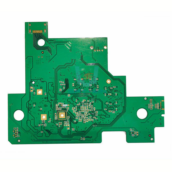
Sky Win PCB Printed Circuit Board Fabrication
Sky Win PCB is one of the leading PCB prototype and turnkey manufacturers located in Shenzhen,China.
We have over than 8 years experience focusing on quick-turn-around printed circuit board manufacturing and can supply more than 50 countries with superior quality and high technology products.
We have complete quality and environment systems of PCB manufacturing, PCB design and SMT after few years of exploding and developing, and become a competitive PCB/PCBA supplier famous for her high technology and effective management.
PCB Fabrication Application
Aerospace & Defense
Automotive PCBs
Healthcare & Medical Devices
Industrial Manufacturing
PCB Assembly Technical Capabilities
| Article | Description | Capability | |
| Sercive | PCB and SMT assembly with one-stop service | ||
| Files we need | PCB: Gerber files(CAM, PCB, PCBDOC) | ||
| Components: Bill of Materials(BOM list) | |||
| Assembly: Pick-N-Place file | |||
| Material | Laminate materials | FR4, high TG FR4, high frequency, alum, FPC | |
| Board cutting | Number of layers | 1-32 | |
| Min.thickness for inner layers | 0.003”(0.07mm) | ||
| (Cu thickness are excluded) | |||
| Board thickness | Standard | (0.1-4mm±10%) | |
| Min. | Single/Double:0.008±0.004” | ||
| 4layer:0.01±0.008” | |||
| 8layer:0.01±0.008” | |||
| Bow and twist | 7/1000 | ||
| Copper weight | Outer Cu weight | 0.5-4 0z | |
| Inner Cu weight | 0.5-3 0z | ||
| Drilling | Min size | 0.0078”(0.2mm) | |
| Drill deviation | ±0.002″(0.05mm) | ||
| PTH hole tolerance | ±0.002″(0.005mm) | ||
| NPTH hole tolerance | ±0.002″(0.005mm) | ||
| Solder mask | Color | Green,white,black,red,blue… | |
| Min solder mask clearanace | 0.003″(0.07mm) | ||
| Thickness | (0.012*0.017mm) | ||
| Silkscreen | Color | white,black,yellow,blue… | |
| Min size | 0.006″(0.15mm) | ||
| E-test | Function Test | 100% Functional test | |
| PCBA Testing | X-ray,AOI Test,Functional test | ||
| Pcb assembly | one-stop service electronic manufacxturer service | ||
| Component sourcing | Yes | ||
| Certificate | IATF16949,ROHS,UL | ||
| Delivery time: | PCB | 3-12days | |
| PCBA | 8-20days | ||
| Tolerance of pcb | ±5% | ||
| Max size of finish board | 450*450mm | ||
| MOQ | NO MOQ (1pcs) | ||
| Surface Finish | HASL,ENIG,immersion silver,immersion tin,OSP… | ||
| PCB outline | Square,circle,irregular(with jigs) | ||
| package | QFN,BGA,SSOP,PLCC,LGA | ||
Typical PCB Fabrication Process
1. Design: The process begins with designing the PCB layout using computer-aided design (CAD) software. This includes placing components, creating electrical connections, and defining the PCB's dimensions and layers.
2. Design Verification: Before fabrication, the design is verified for errors, such as incorrect connections or design rule violations. Design verification tools are used to ensure the design is ready for fabrication.
3. Gerber File Generation: The design files are converted into Gerber files, which are a standard format for PCB fabrication. These files define the copper traces, pads, and other features of the PCB.
4. Material Selection: The substrate material, often FR-4 fiberglass-reinforced epoxy, is chosen based on the PCB's requirements. Other materials, such as copper foil and solder mask, are also selected.
5. Layer Stackup: For multi-layer PCBs, the layer stackup is determined. It specifies the arrangement and order of the copper layers, insulating layers, and prepreg layers that make up the PCB.
6. Preparing the Substrate: The substrate material is prepared by cutting it to the required size and cleaning it to remove any contaminants.
7. Copper Cladding: Copper foil is laminated onto the substrate to form the conductive layers of the PCB. The copper foil is bonded to the substrate using heat and pressure.
8. Imaging and Etching: A photosensitive layer, called photoresist, is applied to the copper layers. The Gerber files are used to expose the photoresist in the desired circuit pattern using UV light. The exposed areas are chemically developed, and the unmasked copper is etched away to create the copper traces.
9. Drilling: Holes, known as vias, are drilled into the PCB to allow for component mounting and electrical connections between layers. These holes may be plated to ensure conductivity.
10. Plating and Surface Finish: The exposed copper surfaces are plated with a thin layer of a conductive metal, such as tin or gold, to protect them from oxidation and facilitate soldering. This plating process also helps establish electrical connections.
11. Solder Mask and Silk Screen: A solder mask layer is applied to cover the entire PCB, leaving only the copper pads exposed. This layer protects the copper traces and prevents solder bridges. A silk screen layer is applied to print component identifiers, logos, and other markings on the PCB.
12. Electrical Testing: The fabricated PCBs undergo electrical testing to ensure that the connections and circuitry meet the design specifications. This testing can include checks for continuity, resistance, and insulation between different layers.
Once the PCBs pass the testing phase, they are ready for component assembly, which involves soldering the electronic components onto the board using PCB assembly processes.It's important to note that the specific details of the PCB fabrication process may vary depending on factors such as the complexity of the design, the desired specifications, and the chosen fabrication facility.
![]()
Send your inquiry directly to us